

With the development of artificial intelligence, AI devices need to integrate more functional modules, such as image processing, speech recognition, natural language processing, etc., in order to meet the high requirements of AI algorithms for computing power, in order to adapt to the high-performance requirements of AI devices, packaging materials also need to be continuously improved to improve their electrical conductivity, thermal conductivity and mechanical strength, and ensure the stability and reliability of the equipment. This article will explore the impact of AI applications on semiconductor packaging and test needs in 2025 and how the industry can address this challenge.
Continuation of technology trends and market demand
Technology trends emerging in 2024, such as silicon wafer development and AI applications, are expected to continue until 2025, especially chip design related to high-performance computing. While the global recession, supply chain issues, and socio-economic challenges are likely to impact the industry, demand for AI remains strong, especially in data center applications, driving continued growth in DRAM in GPUs, CPUs, and high-bandwidth memory (HBM).
The need for high-performance computing in data centers, especially for running large language models (LLMs), has become an important driver in the semiconductor industry. As these demands continue to expand, so do the requirements for semiconductor equipment, which in turn drives innovation in packaging and test technology.
HPC device complexities and challenges
High-performance computing devices (HPCs) are one of the challenges of the semiconductor industry due to their complexity and high level of integration. To improve speed and performance, engineers integrate billions of transistors into chips and use heterogeneous integration techniques to package multiple ICs on the same substrate. This makes HPC devices extremely complex in terms of transistor density, component diversity, and processing requirements.
This complexity makes the equipment susceptible to overheating and mechanical failure. Different components have different power consumption, operating speeds, and thermal management requirements, which greatly increases the difficulty of system design and testing. To address these challenges, the industry is pushing for new packaging technologies and efficient thermal solutions.
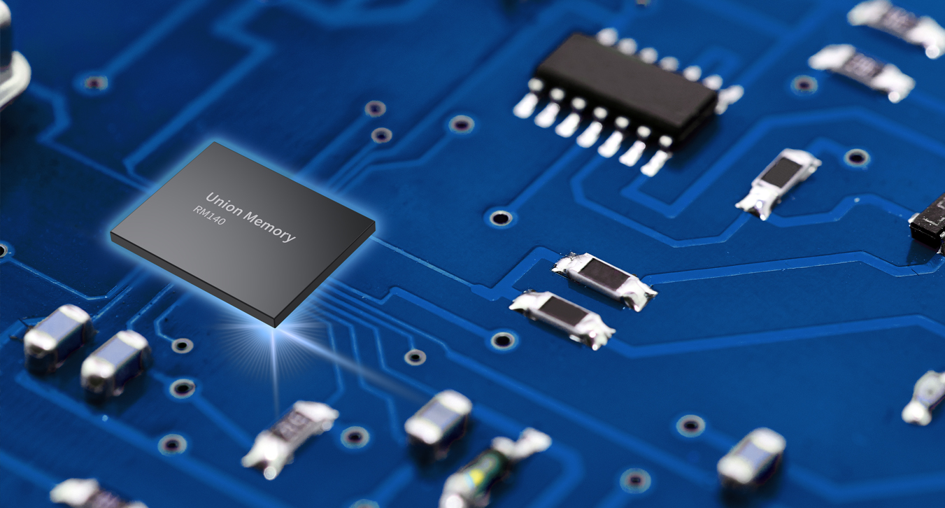
Figure: Artificial intelligence and device complexity will continue to drive packaging and test demand
Increased power consumption and test requirements
With the exponential growth in the power consumption of HPC devices, how to effectively manage and test the power consumption of these devices becomes a critical issue. Test equipment requires a high current supply and advanced thermal control capabilities to ensure the stability of the equipment under high loads.
In addition, to ensure reliability when running large language models (LLMs) in data centers, semiconductor manufacturers must increase test insertion and fault coverage during the manufacturing process. These increased test requirements involve multi-dimensional inspection from the chip to the system level, including system-level testing and burn-in insertion. Test equipment must not only meet the traditional reliability testing requirements, but also support high-complexity AI chip testing.
Industry response and outlook
In the face of the continuous growth of AI demand in 2025, the testing demand of the semiconductor industry will also show an increasing trend. Test equipment vendors, such as Advantest, are responding to these challenges and providing innovative test solutions. Advantest's solutions are designed to handle the high complexity of HPC devices and support efficient testing in different application scenarios.
With the increasing complexity of AI and ML application products, especially the introduction of generative AI in consumer products such as smartphones and laptops, the semiconductor products of the future will be more complex than ever. The increased demand for testing will drive the industry to innovate to meet increasingly stringent technical requirements.
Conclusion
In 2025, as the demand for AI and device complexity continues to increase, the field of semiconductor packaging and test will usher in more challenges and opportunities. The industry must accelerate the pace of technological innovation and improve the accuracy and efficiency of packaging and test technology to meet the growing market demand. Only through more advanced test solutions and continuous technological breakthroughs can we ensure that the semiconductor industry is on track to move forward in the wave of artificial intelligence.


