

Applied Materials, Inc. today announced a new defect detection system designed to help leading semiconductor manufacturers break through the technical bottleneck of chip size scaling. The SEMVision H20 system combines the industry's most sensitive electron beam (eBeam) technology with advanced AI image recognition to detect nanoscale defects deep in leading-edge chips more efficiently and accurately.
Electron beam imaging has long played a key role in detecting tiny defects that are difficult to detect optically. With its ultra-high resolution, it pinpoints subtle defects in billions of nanoscale circuit patterns. In the traditional inspection process, the wafer is typically scanned optically for potential defects, and then analyzed in detail with the help of electron beam technology. However, as chip manufacturing enters the "Angstrom era", the minimum feature thickness of chips is only a few atoms in size, and it becomes increasingly difficult to discern true defects and false positives. In today's most advanced chip process nodes, optical inspection generates a denser defect spectrum, potentially increasing the number of potential defects delivered to beam inspection by a factor of 100. As a result, process control engineers urgently need an inspection system that can handle large sample volumes while maintaining speed and sensitivity in large-scale production.
Keith Wells, Group Vice President, Imaging & Process Control, Applied, said, "The SEMVision H20 system enables the world's leading chipmakers to sift through the vast amounts of data generated by their inspection tools. By combining advanced AI algorithms with the high-speed, high-resolution advantages of innovative electron beam technology, the system can quickly identify small defects deep in the structure of 3D devices, providing faster and more accurate inspection results, thereby shortening factory cycle times and improving yields.”
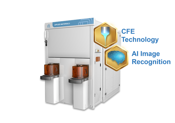
Figure: Applied Materials unveils next-generation electron beam system to accelerate chip defect inspection
Applied's new electron beam technology is critical to the complex three-dimensional architectural changes required to manufacture logic chips for 2nm and beyond, such as surround gate transistor technology, as well as the production of higher-density DRAM and 3D NAND memory. The SEMVision H20 defect detection system is now being used by leading logic and memory chip manufacturers at emerging technology nodes.
The SEMVision H20 system relies on two innovative technologies to achieve high accuracy in defect classification and inspection up to three times faster than existing advanced technologies.
Next-Generation Cold Field Emission (CFE) Technology: Applied's CFE technology is a major breakthrough in electron beam imaging, enabling sub-nanometer resolution to effectively identify subtle defects in the depths. The technology works at room temperature to produce a narrower electron beam with a higher number of electrons, delivering up to 50% better nanoscale image resolution and up to 10 times faster imaging speed than traditional thermal field emission (TFE) techniques. With the introduction of the SEMVision H20, Applied Materials brings the second generation of CFE technology to further increase detection throughput while maintaining industry-leading sensitivity and resolution. Faster imaging speeds increase inspection coverage on a per-wafer basis, enabling chipmakers to obtain the same amount of information in one-third of the time.
Deep Learning AI Image Model: SEMVision H20 leverages deep learning AI capabilities to automatically extract real defects from fake "noise" defects. Applied Materials' proprietary deep learning network, which is continuously trained on data from the chipmaker's factory, can classify defects into dozens of types, such as voids, residues, scratches, and particles, to achieve more accurate and efficient defect characterization.
The SEMVision family of products is the world's most advanced and widely used electron beam inspection system. The combination of next-generation CFE technology and advanced AI models further strengthens SEMVision H20's leading position, enabling chipmakers to accelerate chip development and better apply electron beam technology in mass production.


