

ASML, the world's leading semiconductor equipment manufacturer, plans to deliver the first modules of its second-generation high-numerical aperture (High-NA) extreme ultraviolet (EUV) lithography machine, the TwinScan EXE:5200, in the coming months. This progress marks a major breakthrough in semiconductor manufacturing technology, with the goal of mass production in 2026.
The introduction of high numerical aperture extreme ultraviolet lithography (HPE) technology has enabled chipmakers to achieve smaller feature sizes and higher transistor densities in a single exposure. Compared to traditional low-NA EUV technology, high-NA EUV technology improves resolution from 13nm to 8nm, enabling the creation of smaller, more powerful chips. This is critical to driving the development of cutting-edge technologies such as artificial intelligence, high-performance computing, and autonomous driving.
How it works
Generation of EUV light sources
At the heart of an EUV lithography machine is its light source. ASML's high-NA EUV system uses laser-generated plasma (LPP) technology to produce extreme ultraviolet light. Specifically, the system ejects liquid tin droplets with a diameter of about 25 microns at a speed of 70 meters per second. These tin droplets are first hit by a low-intensity laser vein, which turns it into a pancake-shaped, and then by a more powerful laser vein, creating a plasma and emitting EUV light with a wavelength of 13.5 nanometers. This process is repeated 50,000 times per second to produce enough light for chip fabrication.
Capture and reflection of light
Since EUV light is absorbed in the air, the EUV system operates in a vacuum chamber. Special multilayer mirrors (consisting of alternating layers of silicon and molybdenum) are used to capture and reflect EUV light. These mirrors have extremely high reflectivity and surface accuracy, ensuring precise control of light. These mirrors are manufactured with extreme precision, with a maximum deviation of only 0.1 mm if the surface is scaled up to the size of Germany.
Gobographic projection
The captured EUV light is projected onto a silicon wafer coated with photoresist through a photomask. The photomask is engraved with a pattern of the circuit design, with the transparent part allowing EUV light to pass through, while the other part blocks the light. The light passing through the photomask forms a circuit pattern on the silicon wafer.
Photoresist exposure and development
The photoresist on the silicon wafer undergoes a chemical change when exposed to EUV light, resulting in a change in its solubility in the developer. After development, the patterned photoresist transfers the pattern of the circuit design to the silicon wafer.
Repeated exposure and multi-layer manufacturing
Manufacturing modern chips requires building multiple layers of circuitry on silicon wafers, which often requires multiple iterations of the EUV lithography process, each time using a different photomask to fabricate a different chip assembly.
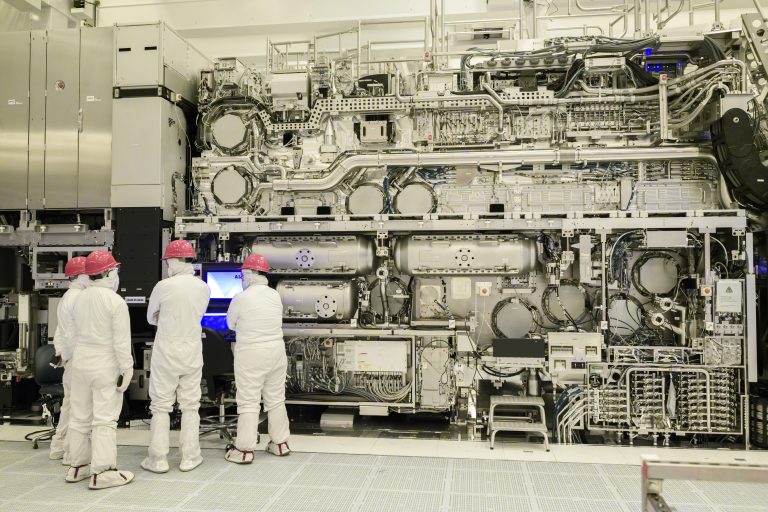
Figure: ASML is about to deliver the second generation of high numerical aperture extreme ultraviolet lithography machine
Technical Features & Benefits:
Higher Numerical Aperture (NA)
At the heart of the high NA EUV technology is its 0.55 NA numerical aperture, which enables smaller feature sizes and higher transistor densities compared to the conventional 0.33 NA. This enables chipmakers to create smaller, more complex chip structures in a single exposure.
Faster wafer and mask tables
Since the exposure field of a high-NA EUV system is only half the size of a conventional EUV system, more exposures are required to complete the patterning of individual wafers. To meet this challenge, ASML has developed faster wafers and mask stages. The wafer stage acceleration capability of the EXE system reaches 8g, which is twice that of the NXE system. The mask table accelerates to 32 g, which is equivalent to a car accelerating from 0 to 100 km/h in 0.09 seconds. These improvements enable the TwinScan EXE:5000 to process more than 185 wafers per hour.
Cost efficiency and simplified manufacturing
High NA EUV technology not only improves resolution, but also simplifies the manufacturing process. Whereas traditional low-NA EUV technology requires the use of sophisticated multiple exposure techniques to achieve high resolution, high-NA EUV technology can be done in a single exposure, reducing production time and cost.
Future outlook
ASML's high-NA EUV technology not only brings significant improvements to current chip manufacturing, but also lays the foundation for future chip architectures. Starting with 2nm logic nodes, high NA EUV technology will support higher density storage nodes. In addition, ASML is also exploring the development of an ultra-NA EUV machine with a numerical aperture of 0.75, which will further advance the development of chip manufacturing technology.
In short, the launch of ASML's second-generation high-NA EUV lithography machine not only marks a major progress in semiconductor manufacturing technology, but also provides solid technical support for the development of the global digital economy.


