

Researchers in Korea have recently made breakthroughs in semiconductors, developing a new p-type semiconductor material and thin-film transistor that is expected to greatly improve the overall performance of next-generation displays and ultra-low-power semiconductor devices.
The Electronic Telecommunications Research Institute (ETRI) has successfully developed a p-type transistor composed of a selenium-tellurium (Se-Te) alloy. The transistors are made of chalcogenide-based p-type semiconductor materials that can be easily deposited at room temperature in a simple process. In addition, the researchers have innovatively designed a new technology to achieve systematic adjustment of the threshold voltage of n-type transistors by controlling the charge injection of tellurium films in the heterojunction structure of n-type oxide semiconductors and p-type tellurium (Te).
The research has been pressed on ACS Applied Materials & Interfaces.
Semiconductors are divided into two categories, intrinsic and non-intrinsic, according to their doping state. In simple terms, intrinsic semiconductors are "pure" semiconductors that are free of impurities. In the case of commonly used silicon materials, there are no free electrons in pure silicon, so it does not conduct electricity even when a voltage is applied. To enhance electrical conductivity, impurities are often introduced into intrinsic semiconductors, and different impurities form n-type or p-type semiconductors.
At present, n-type oxide semiconductors based on IGZO (indium gallium zinc oxide) are widely used in the display industry. However, compared with n-type oxides, p-type semiconductors have poor processing and electrical properties, and low-temperature polysilicon (LTPS) is mainly used as the material. However, LTPS has problems such as high manufacturing costs and limited substrate size.
With the advancement of display technology, especially under the development needs of high refresh rate (above 240Hz) and ultra-high-definition display (8K*4K), the research of p-type semiconductors has gradually attracted more attention. Existing n-type semiconductors have certain limitations in realizing these high-performance displays, so the demand for p-type semiconductors is also increasing.
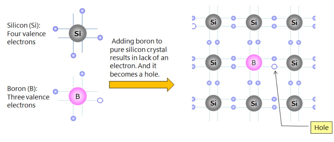
Figure: P-type semiconductors (Source: Toshiba Semiconductor)
To meet this need, the ETRI research team developed a new type of p-type semiconductor by adding tellurium to selenium, increasing the crystallization temperature of the channel layer, and depositing amorphous thin films at room temperature. After heat treatment, the thin film crystallizes and exhibits a higher mobility and switching current ratio than existing transistors.
The researchers also found that the introduction of Te-based p-type semiconductors into n-type oxide semiconductor films to form heterojunction structures can adjust the electron flow and threshold voltage of n-type transistors by controlling the thickness of Te. This structure improves the stability of n-type transistors without the need for a passivation layer.
These technological breakthroughs are expected to drive the display industry toward higher resolution and lower power consumption. In fact, this new technology not only has a significant impact on the display industry, but may even redefine the semiconductor industry landscape. Currently, global semiconductor manufacturers are working to increase integration through miniaturization processes, but as integration approaches its limits, new integration approaches become even more important.
An emerging integration technology is through-silicon vias (TSVs), which involve stacking multiple wafers and drilling holes in them to achieve electrical connections. TSVs offer advantages in terms of space utilization and reduced power consumption, but still face challenges such as high process costs and low throughput.
In response to the limitations of TSV, the industry has proposed monolithic three-dimensional (M3D) integration technology that stacks materials on a single wafer. However, due to the limitations of the high-temperature process, M3D technology has not yet been commercialized. The p-type semiconductors and heterojunction thin-film transistors developed by ETRI are expected to promote the commercialization of M3D technology by being able to operate stably at temperatures below 300°C.
Cho Sung-Haeng, principal researcher at ETRI's Flexible Electronics Research Division, noted that this technological breakthrough has far-reaching implications for the research of future next-generation displays such as OLED TVs and XR devices, as well as other fields such as CMOS circuits and DRAM memory.
Looking ahead, the research team plans to further optimize Te-based p-type semiconductors for substrates of 6 inches or larger, and explore their potential for use in more circuits to advance commercialization and explore new applications.


