

The article I want to share with you today comes from a professional semiconductor industry information platform. The author of the article is an experienced technical editor who has been rooted in the semiconductor field for a long time, and continues to track the cutting-edge trends of the industry with deep professional knowledge and rich industry experience. With keen insight and accurate analysis capabilities, the team has unique insights into semiconductor manufacturing technology, market trends, etc., and has provided many valuable views and suggestions for the development of the industry. This article focuses on the development status, challenges and future trends of extreme ultraviolet lithography (EUV) technology in the field of semiconductor manufacturing, which is of great reference value for the entire semiconductor industry. The following is the core content of the article:
At present, the rapid development of artificial intelligence has triggered an exponential increase in the demand for AI chips. This growth has led to a surge in demand for advanced process chips, which are highly dependent on EUV lithography technology. Currently, only five semiconductor manufacturers – TSMC, Samsung, Intel, SK hynix, and Micron – have achieved mass production of EUVs worldwide. Although Rapidus in Japan has installed ASML's EUV scanner and plans to start mass production in 2027, it will be difficult to alleviate the tight supply-demand situation in the short term. It is predicted that the AI chip market will grow by at least 10 times in the next 5-7 years, such as TSMC's 2nm process orders have been scheduled until 2026, the problem of insufficient EUV production capacity is becoming more and more prominent, ASML's order backlog is serious, and the contradiction between supply and demand needs to be solved urgently.
In terms of technological development, EUV faces many bottlenecks that need to be broken through. At the equipment level, its high cost and complex process have become insurmountable obstacles for many manufacturers. To address this, government-backed research centers, such as imec in Belgium and EUV Accelerator in the United States, have joined forces to invest in R&D to improve mask technology, optimize process control, and improve photoresist chemistry. At the same time, strategies such as hybrid lithography (EUV for critical layers, other lithography techniques for non-critical layers) and multiple patterning (such as double patterning and quadruple patterning) have been widely adopted, which not only reduces costs, but also allows deep ultraviolet lithography (DUV) to continue to play a role in some scenarios. Some companies are also exploring nanoimprint lithography (NIL) and self-assembly patterning technologies to provide new possibilities for the manufacture of specific layers.
Masks and photoresists are critical aspects of EUV technology, but they also present a number of challenges. Unlike the transmissive masks used in traditional DUV lithography, EUV masks are reflective, and even the slightest defect can lead to patterning failures, which can greatly impact production yields. Researchers have responded by improving multi-beam mask writers, developing highly transparent protective film technology, and pursuing defect-free mask substrates, although some progress has been made, such as multi-beam electron beam mask writing technology to improve mask production efficiency and accuracy, and new carbon-based protective films to improve thermal stability and transmittance, but the cost of masks remains high.
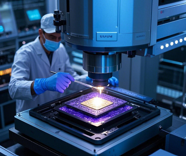
Figure: EUV lithography, the future of semiconductor manufacturing or the thorny road?
Photoresist materials are also a key challenge in achieving high yield and process stability for EUV lithography. Chemically amplified photoresists (CARs) have been the industry standard for decades, but at advanced process nodes, acid diffusion and random defects make it difficult to meet the stringent requirements of next-generation semiconductor manufacturing. Metal oxide photoresists (MORs) have the advantage of strong absorption at EUV wavelengths and high contrast at low thickness, but their sensitivity to process conditions and high dose requirements limit their application. Multi-trigger photoresists (MTRs) use smaller molecules to achieve smaller feature sizes and higher resolutions, but there are areas for continuous improvement, such as process compatibility. In addition, the defect problem of photoresist directly affects the feasibility of EUV in large-scale production, and the reduction of defect rate has become the focus of research, and with the continuous reduction of the thickness of the bottom layer, the requirements for molecular-level control of photoresist are becoming more and more stringent.
The good news is that AI and machine learning technologies are opening up new opportunities for EUV. AI-driven metrology tools developed by companies like Tignis and Synopsys can analyze process variations in real time and dynamically adjust scanner parameters such as exposure dose, alignment tolerances, and photoresist baking conditions to reduce production variability. Machine learning models can also learn from large amounts of wafer data to identify random defect trends and propose corrective actions in advance, which not only accelerates the EUV development cycle, but also improves production efficiency and product quality.
The light source is one of the most important factors in the cost structure of EUV lithography. EUV lithography relies on a high-energy laser source to produce 13.5nm extreme ultraviolet light, but existing light sources are extremely inefficient, and a lot of energy is lost before it reaches the wafer. ASML's latest-generation scanners consume hundreds of kilowatts of power per system, making them costly. To address this issue, Lawrence Livermore National Laboratory (LLNL) is developing diode-pumped solid-state lasers (DPSSLs) that are more power-efficient and consume less power than traditional CO₂ lasers, potentially reducing the cost per wafer produced. Okinawa Institute of Science and Technology (OIST) focuses on optimizing the use of photons inside scanners by improving mirror coatings and reducing optical aberrations to increase the amount of light reaching the wafer, thereby improving tool efficiency and shortening exposure times.
From the perspective of application expansion, innovative business models and infrastructure strategies are essential to promote the adoption of EUV technology in more semiconductor manufacturers. On the one hand, the shared EUV infrastructure of research centers such as imec and EUV Accelerator provides fabless and small foundries with access to and use of EUV technology. On the other hand, the foundry model, which draws on the chiplet strategy and focuses on the production of specific types of chiplets such as I/O chips and memory chips, is expected to lower the threshold for the application of EUV technology and benefit more manufacturers.
EUV lithography is of great significance in the field of semiconductor manufacturing, and its future development is full of opportunities and challenges. The semiconductor industry needs to make breakthroughs in many key areas such as photoresist materials, process control, and light source technology, while actively exploring new business models and manufacturing models, in order to fully unleash the potential of EUV technology and promote the semiconductor manufacturing industry to a new stage of development.


