

In extreme environmental applications such as aerospace, nuclear power, and high-energy particle detection, electronic devices face severe irradiation challenges. Traditional silicon devices are prone to functional failure or even permanent damage in strong irradiation fields, and more alternative material systems are urgently needed. With the mature application of silicon carbide (SiC) as a third-generation semiconductor material, its excellent performance in anti-radiation scenarios has attracted great attention around the world. In this paper, China Exportsemi will start from the basic physical mechanism of silicon carbide materials, analyze the technical principles and testing research progress of its radiation resistance, and discuss its application prospects and localization opportunities in extreme environments.
Ⅰ. The strategic significance of anti-irradiation electronic devices
In space orbit, near-Earth satellites, and deep space exploration missions, electronic devices will be exposed to high-intensity cosmic rays such as protons, electrons, and heavy ions for a long time. In nuclear reactor control systems and high-energy particle collision experimental devices such as CERN, neutrons and γ rays also pose a serious threat to electronics. These emissions can cause device parameter drift, breakdown, soft errors, and even permanent failure.
Therefore, electronic devices with anti-radiation ability are not only the key support for aerospace and nuclear energy engineering, but also related to mission safety and the stable operation of national strategic projects. In this context, material systems with higher radiation resistance are gradually replacing traditional silicon devices, among which silicon carbide is emerging.
Ⅱ. Silicon carbide material characteristics and anti-irradiation machine
Silicon carbide (SiC) is a wide bandgap semiconductor material with a bandgap width of about 3.26 eV (4H-SiC), which is much higher than that of silicon (1.12 eV). This physical property gives it higher resistance to thermal and voltage breakdown, in addition to excellent radiation resistance. Fundamentally, the covalent bond energy between carbon and silicon is about 45 eV, which is more than twice that of silicon, which makes its atomic structure less prone to displacement damage when hit by high-energy particles.
The effects of radiation on semiconductor materials are mainly reflected in two aspects:
* Ionization effect: High-energy particles excite electron-hole pairs, causing device threshold drift and leakage current rise.
* Non-ionizing energy damage (NIEL): Particles hit lattice atoms, causing dislocations and vacancies, affecting carrier mobility and lifetime.
Compared with silicon devices, silicon carbide shows stronger inhibition ability in the face of the above two effects. For example, the variation of the main electrical parameters (such as threshold voltage and switching performance) of SiC devices after irradiation is much smaller than that of Si devices, and the soft error rate is also lower, which is the physical basis for its application in the field of space and nuclear energy.

Figure: Technical analysis and industry analysis of the radiation resistance of silicon carbide devices
Ⅲ. Research progress on anti-radiation of silicon carbide devices
In recent years, many institutions at home and abroad have carried out systematic irradiation tests on silicon carbide devices. NASA and Air Force Research Laboratory (AFRL) conducted γ-ray and proton beam irradiation tests on 1200V SiC MOSFETs as early as 2015, and the results showed that the device remained functionally stable at the cumulative dose of 10^12 rad (Si) level, and the gate voltage drift was less than 10%.
The European Space Agency (ESA) has also conducted multiple rounds of irradiation tests to verify the reliability of SiC JFETs and PIN diodes in high-energy electronic and heavy ion environments. More importantly, the self-recovery ability of some SiC devices after irradiation shows strong potential, reflecting their practical value in the "recyclable deep space electronics platform".
Domestically, the Institute of Microelectronics of the Chinese Academy of Sciences and the China Institute of Atomic Energy have also made progress in the research on irradiation of SiC devices. As shown in the study released in 2022, the domestic 1200V SiC MOSFET still maintains normal switching capability after 10^13 n/cm² fast neutron irradiation, and only the gate leakage current increases slightly. This shows that domestic devices have gradually approached the international advanced level in key indicators.
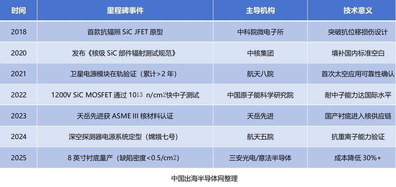
Figure: R&D milestones of domestic SiC anti-irradiation devices (2018–2025)
Ⅳ. Key application scenarios and landing challenges
The radiation resistance of silicon carbide devices makes it a great potential in the following areas:
* Spacecraft power supply system: including power conversion module, attitude control circuit, etc., which still needs to operate stably in a high-energy ion environment;
* Deep space exploration and planetary landers: facing far-earth orbit or the far side of the Moon, they need to withstand extreme temperatures and radiation;
* Nuclear reactor instrumentation and control system: control electronics need to maintain long-term operation in a high-dose neutron environment;
* High-energy particle detection experiments: such as particle colliders, signal front-end reading circuits in synchrotron radiation devices.
However, there are still several challenges for SiC devices to achieve large-scale engineering applications:
* Manufacturing consistency problem: wafer defect density has a significant impact on the performance stability after irradiation;
* The standard system is not perfect: there is a lack of unified international specifications for the evaluation of SiC devices against radiation;
* Cost issues: Silicon carbide substrates and devices are still at a relatively high price point, which affects the penetration of low-cost projects.
Ⅴ. The industrial layout of domestic silicon carbide anti-irradiation devices
With the support of the national "14th Five-Year Plan" major special projects, domestic R&D investment in the anti-radiation capability of SiC materials and devices continues to increase.
* The anti-irradiation power device project led by the Institute of Microelectronics of the Chinese Academy of Sciences has completed the verification of MOSFET and diode devices of multiple power levels;
* The technology accumulation of SICC, Tanke Blue, San'an Optoelectronics and other enterprises in the field of power devices provides a device foundation for anti-radiation applications;
* End-user units such as the Fifth Academy of Aerospace Science and Technology and China National Nuclear Corporation have begun to test the performance of domestic SiC devices in satellite and nuclear engineering in small batches.
In the future, if domestic SiC devices can take advantage of the technological differentiation advantage of "high radiation tolerance", they are expected to open an export window in the international aerospace and nuclear engineering equipment market.
Ⅵ. Conclusion and outlook
Silicon carbide is not only the "star material" of new energy vehicles and industrial power supplies, but also has irreplaceable strategic value in the field of radiation resistance. Its physical properties determine its superior performance in extreme environments, gradually changing the previous perception of the performance limit of silicon materials.
With the continuous optimization of radiation-resistant SiC devices, the establishment of domestic standard systems, and the continuous promotion of supply chain localization, we have reason to believe that silicon carbide will play a "cornerstone role" in the future core mission electronic systems in higher irradiation and more complex environments. In the next ten years, it will be one of the key paths for semiconductor material technology to climb the "peak".


