

Reading guide: This article is GigaDevice's technical contribution to China Exportsemi, focusing on its latest release of 500W single-stage photovoltaic microinverter solution. In response to the urgent demand for high efficiency, high integration and low cost in the global distributed PV market, the solution is built based on GigaDevice GD32G553 MCUs and Navitas GaN power devices, and comprehensively improves the performance and reliability of PV inverter systems through system-level architecture optimization and high-precision control. This paper deeply analyzes its architectural advantages, control strategies and key performance indicators, and fully demonstrates the innovation ability and overseas competitiveness of China's local semiconductor enterprises in the field of new energy power electronics.
Driven by the "dual carbon" goal, distributed photovoltaic has become an important carrier of energy transformation due to the advantages of flexible deployment. As the core equipment of DC to AC of photovoltaic modules, microinverters can effectively solve the mismatch loss and safety problems of traditional string solutions by virtue of module-level precise control, and their value is prominent in residential and building-integrated photovoltaic (BIPV) scenarios. With the industry's demand for high integration, high efficiency and low cost, the single-stage architecture is leading the technological revolution of microinverters with its minimalist design and high performance.
GigaDevice is deeply engaged in the semiconductor field, and officially launched a single-stage microinverter solution based on high-performance GD32G553 MCUs according to the hot spots in the photovoltaic industry, which adopts a one-in-one architecture and has the advantages of high efficiency, low loss, high integration and cost optimization, which can meet the application needs of users in distributed photovoltaic systems in terms of intelligent operation and maintenance, system reliability and other aspects, and help photovoltaic microinverter solutions develop in a more intelligent, integrated and low-carbon direction.
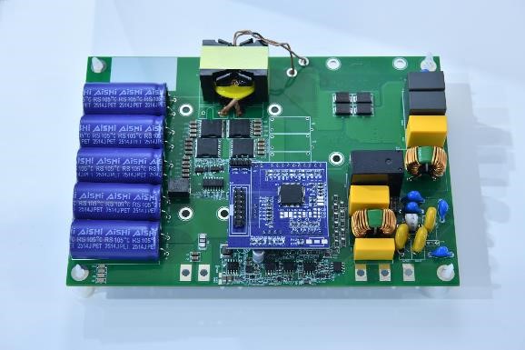
Figure: GigaDevice 500W single-stage photovoltaic microinverter solution display board
Ⅰ Innovate on a single-level architecture
As an energy conversion device that is directly integrated on the back of a single block or a small number of PV modules, the core technical advantage of microinverters lies in their unique module-level maximum power point tracking (MPPT) function. This feature enables it to maximize system power generation by independently optimizing the power output of each module in scenarios of performance differences between modules or local shading. At present, it is widely used in scenarios that require high flexibility and security, such as household distributed photovoltaic systems and building-integrated photovoltaic (BIPV).
According to the different circuit structures, microinverters are mainly divided into two architectures: two-stage and single-stage. Compared with the traditional two-stage architecture, the single-stage architecture has become the main direction of industry technology evolution due to its higher energy conversion efficiency, simpler BOM and lower manufacturing cost. GigaDevice's 500W single-stage microinverter solution adopts a single-stage, one-in-one, architecture based on GD32G5 series MCUs and Navitas' bidirectional GaNFast GaN power ICs, which embodies the core advantages of this technology direction.
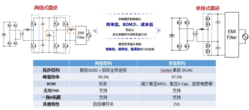
Figure: Comparison of single-stage and two-stage inverter architectures
The single-stage architecture simplifies the circuit structure and improves efficiency by eliminating the need for a first-stage DC-DC conversion. It is worth noting that, on the basis of realizing the core function of microinverter, this architecture also supports reactive power THD optimization and one-to-n expansion to meet the technical requirements of different application scenarios.
The single-stage topology is mainly composed of a primary-side full-bridge circuit, a transformer, a secondary-side half-bridge circuit, and an EMI filter circuit. Through the synergy between the primary side phase shift control and the secondary side phase shift control, the voltage at both ends of the transformer leakage inductance is adjusted, and then the size of the leakage inductance current is controlled to achieve efficient power transmission control. In order to meet the needs of wide voltage gain and power transfer ratio in microinverter applications, it is difficult for a single modulation mode to balance the dual goals of power transfer range and efficiency optimization. The hybrid modulation mode dynamically switches the modulation mode through soft switching and power transmission conditions, which effectively reduces the reflow power and expands the soft switching range while ensuring the given power transmission target, so as to meet the requirements of high-efficiency energy transmission and high-quality grid connection.
At the technical implementation level, it is easy to have problems such as wave loss and continuous wave in the process of phase shift control. GigaDevice GD32G553 MCUs provide a perfect solution to the above problems with high-precision and high-flexibility high-precision timer (HRTIMER) peripherals, and functions such as phase-shifting, counting, reset, and synchronous update between carriers. At the same time, the GD32G553 MCU has powerful computing power, flexible PWM wave generation mechanism and abundant analog peripheral resources, which meet the strict requirements of single-stage micro-inverter in wave transmission, sampling and loop control, and ensure the stable operation of single-stage micro-inverter under complex working conditions.
Ⅱ Full-link control architecture and system-level optimization design
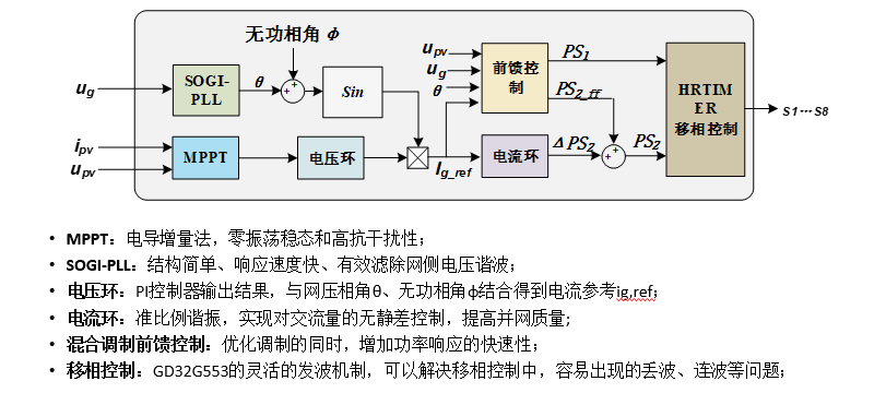
Figure: Block diagram of GigaDevice's 500W single-stage microinverter control scheme
In the system control architecture, the MCU is GD32G553 as the core control unit, which is responsible for PWM generation, signal sampling, and loop control. The secondary power conversion section uses Navitas' bidirectional BDS GaN power devices. The whole control loop is as follows: firstly, the PV voltage reference value is calculated by the maximum power point tracking (MPPT) algorithm, and the dynamic tracking of the PV voltage reference value is realized by the voltage loop controller; The results obtained from the voltage loop calculation are combined with the grid voltage phase information extracted from the SOGI PLL phase-locked loop and the given reactive power phase angle information to provide a current reference for the feedforward controller and the current loop controller. Finally, the primary and secondary side-shift controls were calculated and converted into actual driving pulses through the high-precision timer module to achieve precise control of the power circuit.
In the MCU implementation process, the control algorithm is mainly composed of four parts: phase-locked loop, feedforward compensation, closed-loop control and phase shift conversion, and the execution time of these parts is tested, and the results show that the GD32G553 controller shows good computing performance.
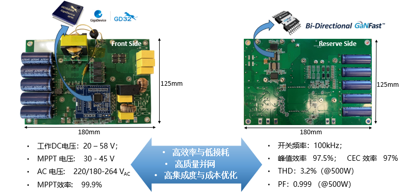
Figure: Performance indicators of GD32G553 series MCUs and Navitas' bidirectional BDS GaN power devices
Through system-level optimization, the whole solution has the characteristics of high efficiency, high-quality grid connection and high integration: at 100kHz switching frequency, it achieves 97.5% peak efficiency and 97% CEC weighted efficiency, and MPPT efficiency is 99.9%; At 500W, the THD was 3.2% and the PF was 0.999.
First of all, in terms of high efficiency and low losses. ZVS can be realized for all switches, which significantly reduces switching losses; The soft-switching range is broadened by an optimized hybrid modulation strategy. Reduce the return power and transformer current rms value, and reduce the conduction loss; At the same time, Navitas BDS GaN is used to reduce switching losses.
Secondly, in terms of high-quality grid connection. The feedforward control of the scheme can improve the power response speed and strengthen the tracking effect of grid voltage. Closed-loop Q-PR control can track AC signals without static differences, improving the quality of grid-connected current. At the same time, through the collaborative adjustment between the primary and secondary phase shift control quantities, the mode can be switched without disturbance, so as to smooth the transformer current and grid-connected current.
Finally, in terms of high integration and cost optimization. The solution adopts the magnetic integration technology of a transformer with a single integrated inductor to reduce the volume of the magnetic component, and uses bidirectional BDS GaN to meet the demand for bidirectional switches on the AC side, which further reduces the size and the overall BOM cost of the solution.
Ⅲ Create a rich product matrix and build a high-quality ecosystem
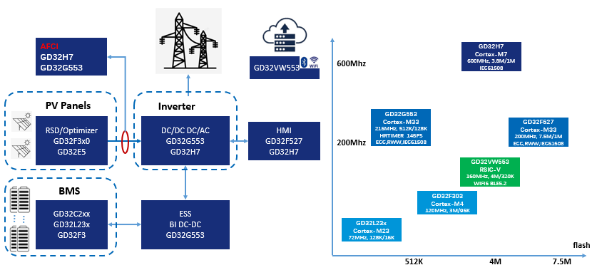
Figure: Application of high-performance GD32 MCUs in the field of digital energy
In the field of new energy control, GigaDevice has built an MCU product matrix covering all scenarios, which is widely used in photovoltaic shutdowns, optimizers, AI arc detection, energy storage ESS systems, BMS, inverters, HMI communication monitoring and other product applications. In the parts of arc pull detection, optimizer, Bi DC-DC, industrial and commercial storage BMS, GigaDevice also provides a complete solution for customers to use directly or secondary development, which can greatly reduce the R&D cycle. In terms of power control, GigaDevice has 600Mhz GD32H7 series and 216MHz GD32G5 series MCUs for customers to choose from.
The GD32G553 used in this solution belongs to GigaDevice's GD32G5 series MCUs. The series has excellent computing power, using Arm® Cortex-M33® core, up to 216MHz, built-in single-precision floating point unit (FPU), as well as hardware trigonometric accelerator (TMU) and other hardware acceleration units. These features dramatically increase data processing speed and complex computing capabilities. At the same time, the GD32G5 series MCUs can support up to 16 channels of high-precision PWM output with a resolution of up to 145ps. It can support variable duty cycle, frequency conversion, phase shift and other wave transmission methods.
In addition to the advantages of computing power and wave control, the GD32G553 also supports four 12-bit ADC modules with a sampling rate of up to 5.3 MSPS and up to 42 sampling channels, which can efficiently collect and process signals from a variety of sensors. At the same time, the GD32G553 is equipped with 8 CMPs (on-chip comparators), which have the characteristics of fast response and flexible configuration, and its output signal can be directly connected to the HRTIMER internally to realize PWM blocking or switching.
In addition to creating high-performance products, GigaDevice also strengthens ecological construction. GigaDevice and Navitas have jointly established a joint R&D laboratory to integrate GigaDevice's high-computing power MCUs and Navitas' high-frequency, high-efficiency GaN technology to create intelligent and efficient digital power products, bringing more solution choices to customers. At the same time, with GigaDevice's ecosystem of the whole industry chain and Navitas' deep understanding of system applications, it will accelerate the layout of AI data centers, photovoltaic inverters, energy storage systems, charging piles, electric vehicles and other fields.


