

The global semiconductor shortage in 2020-2022 and the ensuing chip war have exposed the risk of over-concentration of supply chains. India, one of the world's largest importers of chips, has suffered greatly from the crisis, but it has also started a transformation from "buyer" to "player". In 2025, with fabs in Gujarat and Karnataka coming online, India is trying to take its place in the Asian semiconductor map with mature processes, packaging and testing and design services.
Three advantages of Indian semiconductors
1. Talent Dividend: From "Silicon Valley Code Farmer" to "Chip Engineer", India trains more than 1.5 million engineers every year, of which thousands are already active in the R&D departments of international semiconductor companies. Tata Group's partnership with Taiwan's Powerchip, and ISMC's joint venture with Israel's Tower Semiconductor, all rely on local talent pools. The Indian Institute of Technology (IIT)'s new semiconductor engineering program further extends the advantages of IT to the hardware field.
2. Compared with the high cost of Taiwan and South Korea, India's labor cost is only 30%-40% of the former. In addition, in the context of the US-China technology game, India, with its democratic form of government and strategic cooperation with the West, has become a "safe haven" for multinational companies. Micron's $2.75 billion packaging fab and Vedanta-Foxconn's $19.5 billion wafer fab project reflect this logic.
3. The strong domestic demand market has driven the Indian government's policies of "defense independence" and "popularization of electric vehicles", which have spawned the demand for local chips. For example, Sahasra Semiconductor's memory chip production line in Noida gives priority to meeting the needs of military and automotive electronics; Kaynes Technology's high-reliability packaging technology is aimed at the aerospace industry.
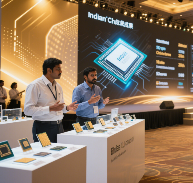
Figure: The rise of semiconductors in India: a breakthrough with both opportunities and challenges
Breakthrough in the industrial chain: a progressive layout from design to packaging
1. Design services: Hidden champions such as Wipro and HCLTech have long provided design services for Qualcomm and NVIDIA, and local fabless start-ups have also emerged under policy incentives. Although high-end IP is still dependent on overseas, India already has the ability to independently design chips above 28nm.
2. Packaging and testing: Micron's test and packaging factory and SPEL's pure OSAT (outsourced packaging and testing) business have enabled India's rapid rise in the ATMP field. The technical threshold of this link is relatively low, but the profit is stable, which is suitable for India's industrial base at this stage.
3. Manufacturing: Vedanta-Foxconn's 28nm factory and ISMC's 65nm analog chip production line are prioritized for mature processes, both of which avoid competition with TSMC and Samsung's advanced processes, and focus on meeting mature market needs such as automobiles and home appliances.
Challenge: Supply chain, technology and infrastructure shortcomings
1. The "glass ceiling" of technology transfer is almost blank in India with a process below 10nm, and technology needs to be obtained through international cooperation. For example, in the Tata Group's partnership with Powerchip, the core equipment is still imported.
2. The "last mile" problem of the supply chain, photoresist, special gases and other key materials rely on imports for 90%, and the localization rate is less than 5%. Although the government plans to build a chemical park, it is difficult to break through in the short term.
3. The "time difference" of hydropower infrastructure Semiconductor manufacturing requires ultra-pure water and stable electricity, while some factories in India are still at risk of power outages of several hours a day. Although Gujarat has accelerated its infrastructure, it will still take 5-10 years to cover the whole country.


