

Moore's Law was once a core driver of the semiconductor industry, but as the manufacturing process approaches its physical limits, the improvement of chip performance is facing unprecedented challenges. In this context, the emergence of silicon photonics technology (SiPh) has injected new hope into the industry. The cooperation between NVIDIA and TSMC has pushed this technology to the focus of the industry and attracted widespread attention. China Exportsemi will delve into the breakthrough of silicon photonics technology, market prospects, and its potential to alleviate the extreme anxiety of Moore's Law.
Breakthroughs and core advantages of silicon photonics technology
Silicon photonics technology uses silicon-based materials to achieve photon transmission, using photons instead of traditional electrons for intra-chip communication, thereby increasing speed and reducing power consumption. This technology offers significant advantages:
1. High-speed communication: Photonic communication can transmit data at a significantly faster speed than electronic communication, making it easy to transfer data to hundreds of gigabits per second, making it suitable for data-intensive applications.
2. Low power consumption: The energy consumption of optical signals is significantly lower than that of electrical signals, especially in high-load environments such as data centers.
3. Higher bandwidth: Silicon photonics technology is able to support large-scale parallel data transmission, which is critical for applications such as artificial intelligence and high-performance computing.
At present, TSMC has made a number of breakthroughs in silicon photonics technology. For example, its 3nm process combined with silicon photonics technology could launch chips that support 1.6T high-speed transmission in 2025. This technology can effectively solve the bottleneck problem of bandwidth and energy efficiency of data centers and AI chips.
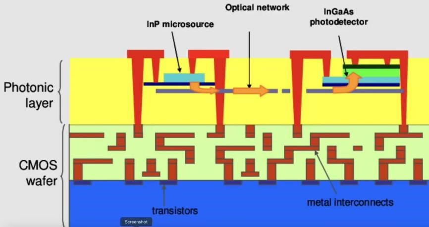
Figure: Schematic diagram of the structure of a silicon photonic chip
Nvidia-TSMC Collaboration: A Combination of Technology and Application
As a leader in the field of AI chips, NVIDIA's cooperation with TSMC, the world's largest wafer foundry, demonstrates the strong combination of technology and manufacturing. Key highlights of this collaboration include:
1. Breakthroughs in advanced packaging technology
TSMC's leadership in co-packaged optics (CPO) technology enables optical modules to be integrated with ASIC or GPU chips, providing a new solution for AI chips. For example, TSMC's latest CPO technology, combined with its wafer-level advanced packaging capabilities, can significantly improve the computing efficiency of AI chips.
2. Acceleration of high-performance computing
NVIDIA's AI chips, with the help of TSMC's silicon photonics manufacturing capabilities, can achieve higher bandwidth and lower latency data communication. This will greatly promote the efficiency of AI training models and further strengthen NVIDIA's market leadership in AI computing.
The impact and potential of silicon photonics on Moore's Law
Moore's Law is based on the assumption that transistors are shrinking, but as the process moves below 2 nanometers, physical limits have become unavoidable. Silicon photonics technology provides a new path for improving chip performance by:
1. Break through the transmission bottleneck: Photonic communication can achieve dozens of times the speed of traditional electronic communication, so that the communication efficiency inside and outside the chip is no longer limited by the physical limitations of traditional wires.
2. Optimized power consumption: The energy efficiency ratio of photonic communication is significantly better than that of electronic communication, especially suitable for high-density computing scenarios.
This makes silicon photonics an important tool for breaking through the limitations of Moore's Law in the future, especially in the fields of AI, high-performance computing, and big data, and its potential applications are immeasurable.
Market outlook and practical challenges
Market outlook
With the rapid increase in the requirements of AI applications for data processing capabilities, the market demand for silicon photonics technology is gradually emerging. According to market research data, the silicon photonics market is expected to grow at a CAGR of more than 25% from 2024 to 2030. In the fields of AI data centers, high-performance computing, and 5G communications, the application of silicon photonics technology will continue to expand.
In addition, silicon photonics technology has a natural advantage in the demand for low-power chips. In the case of data centers, for example, energy consumption has become a central challenge, and the potential of silicon photonic communications to optimize energy efficiency will help the industry move towards green computing.
Real-world challenges
Despite its promising prospects, silicon photonics technology still faces a number of technical and market-to-market obstacles:
1. Production costs
The large-scale manufacturing cost of silicon photonic chips is still high, and how to optimize the process to reduce costs is the key to the popularization of the technology.
2. Ecosystem building
The standardization and equipment compatibility of silicon photonics technology still need to be improved, and the coordinated development of upstream suppliers and downstream application providers in the industrial chain is imminent.
3. Heat dissipation issues
With the improvement of optoelectronic hybrid integration, heat dissipation has become an important factor affecting the reliability of chips, and further innovation in packaging and cooling technologies is required.
Conclusions and future prospects
The rise of silicon photonics technology has provided new ideas for the semiconductor industry to break through the limits of Moore's Law. The cooperation between NVIDIA and TSMC not only pushes silicon photonics technology to the forefront, but also provides strong support for the future development of AI chips.
Looking ahead, silicon photonics technology is expected to become the core driving force for the performance improvement of AI and high-performance computing chips. It is estimated that by 2030, silicon photonics technology will fully penetrate in data centers, AI model training, high-speed communication and other fields, and become one of the basic technologies of the industry. At the same time, the collaboration between NVIDIA and TSMC will become an example of the commercialization of silicon photonics technology, setting a benchmark for the industry.
Driven by technological progress and market demand, silicon photonics technology may open a new era in the chip industry and provide a new direction for the development of the post-Moore's Law era.


