

Resonac Corporation recently announced a major technological breakthrough with the introduction of a new temporary bonding film and debonding process designed to advance semiconductor packaging technology further. Designed for both front-end and back-end processes in semiconductor device manufacturing, this technology not only significantly improves production efficiency, but also ensures a high level of cleanliness throughout the process.
Resonac's new temporary bonding film enables the temporary bonding of wafers or chips to glass carriers during semiconductor device manufacturing to improve process operability. The film is highly heat-resistant and chemically stable, and exhibits sufficient adhesion properties when the wafer or die is temporarily supported on the carrier. What's more, once debonded from the support, the membrane can be easily removed by peeling at room temperature without leaving any residue. In this innovation, this makes the process more efficient while ensuring the purity and integrity of the product.
In contrast to the traditional laser ablation debonding process, Resonac's new debonding method uses xenon (Xe) flash lamp technology. This technology avoids the formation of foreign substances such as oil smoke during the debonding process, and is faster and more applicable than conventional laser processes, not only at the wafer level, but also at the panel level. In addition, xenon flash lamps reduce thermal stress and mechanical damage to wafers or packages, thereby ensuring the integrity and performance stability of semiconductor devices. This process is not only suitable for wafer level, but can also be extended to panel level processing. Compared to conventional laser ablation methods, Xe flash illumination enables debonding in a shorter time while avoiding thermal or mechanical stress damage to the wafer or package.
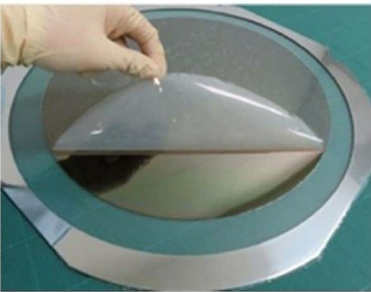
Figure: Resonac develops wafer temporary bonding films and their stripping processes for advanced semiconductor packaging
The technology has already been patented in Japan, United States, Korea, China and Taiwan, and Resonac is seeking development partners to further advance the market application of this innovation. The temporary bonding and debonding process is suitable for memory, logic, and power semiconductors, and is seen as another major breakthrough in semiconductor packaging, especially in the context of the growing demand for high-performance, small-size, low-power packaging solutions.
With this innovation, Resonac is once again demonstrating its important role in driving the advancement of semiconductor technology. As the demand for higher performance, smaller size, and more environmentally friendly packaging technology for future electronic devices continues to increase, this new technology from Resonac is expected to bring a wide range of applications in the future and provide more impetus for the continued growth of the industry.
According to Resonac, this temporary bonding film and novel debonding method is suitable for the manufacturing process of memory, logic and power semiconductors, as well as advanced semiconductor packaging. With the growing demand for high-performance, small-size, and low-power packaging solutions in the semiconductor industry, Resonac's technology is poised to bring a new direction to the industry.


