

In the global semiconductor memory field, the race for NAND flash memory technology is heating up. In order to achieve a leading edge in technology, major storage giants continue to increase R&D investment, strive to break through the limitation of layers, and improve product performance. Recently, according to the latest report from ZDNet, Samsung Electronics plans to adopt China's Yangtze River Storage Technology Co., Ltd. (YMTC)'s patented hybrid bonding technology starting with its 10th generation (V10) NAND flash memory products.
As a leader in the global semiconductor industry, Samsung has long been a leader in NAND flash memory technology. Previously, Samsung used the COP (Cell on Peripheral) method in NAND production, in which peripheral circuits are placed on a wafer and memory cells are stacked on top of it. However, as the number of NAND flash memory layers continues to increase, the stress on the underlying peripheral circuitry beyond 400 layers can affect the reliability of the product. To meet this challenge, Samsung needed to find new technology solutions.
As the largest NAND flash memory manufacturer in China, YMTC has excelled in technological innovation. About four years ago, YMTC pioneered the application of a hybrid bonding technology called "Xtacking" to the production of 3D NAND flash memory and has built a strong patent portfolio around the technology. Even in the face of U.S. sanctions, YMTC still relies on its own R&D strength to make major breakthroughs in technology. According to TechPowerUp's report, YMTC's Xtacking 4.0 (Gen5) process has been successfully applied to its fifth-generation 3D NAND flash memory chips, enabling 294 layers of stacking. This achievement not only reflects YMTC's deep accumulation of NAND flash memory technology, but also demonstrates the tenacity and innovation ability of Chinese semiconductor companies in the face of external pressure.
It is reported that Samsung plans to start mass production of V10 NAND flash memory products in the second half of 2025, which is expected to reach 420 - 430 stacked layers. If implemented, this move will put Samsung in the race for the number of NAND flash memory layers. In addition to Samsung, SK Hynix is also rumored to be negotiating a patent agreement with YMTC. This shows that YMTC's "Xtacking" technology has been widely recognized in the industry and has become a key technology that many enterprises are competing for.
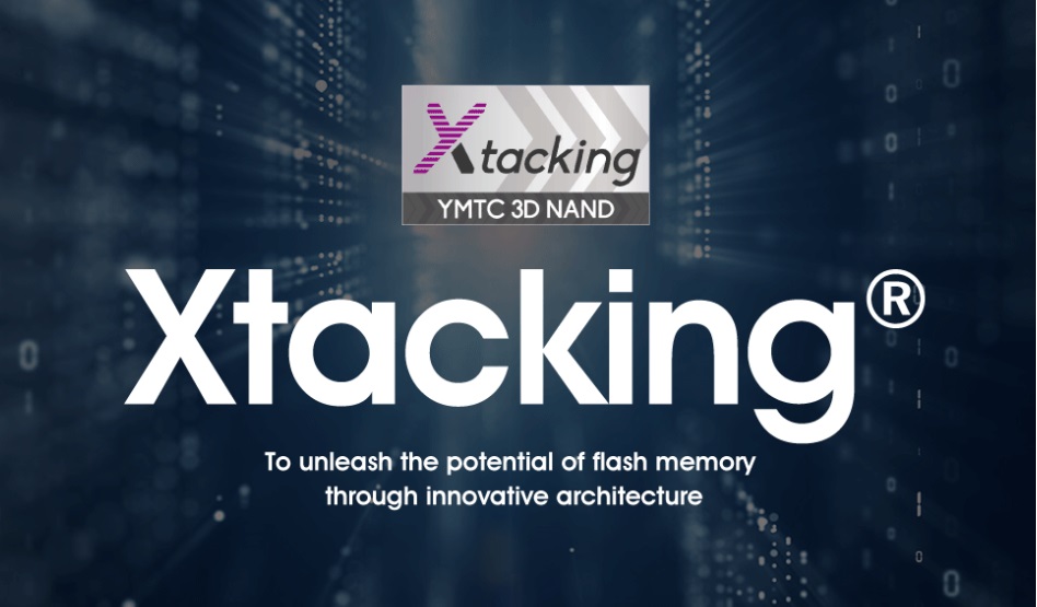
Figure: Samsung may adopt YMTC hybrid bonding patents
In the global NAND flash memory market, the biggest players are accelerating their R&D and pushing the boundaries of higher layers. Currently, Samsung has achieved mass production of 286-layer NAND flash memory in April 2024; SK hynix achieved 321-layer NAND flash production in November 2024 and plans to mass-produce products with more than 400 layers in 2026. Micron will achieve 276-layer NAND flash production in July 2024; Kioxia will achieve 332-layer NAND flash storage in February 2025 and plans to launch 1,000-layer NAND flash memory products in 2027. YMTC achieved 294-layer NAND flash storage in January 2025, and with its "Xtacking" technology, it also occupies a place in this fierce competition.
From an industry perspective, the increase in the number of NAND flash memory layers means higher storage density and lower costs, which is critical to meet the growing demand for data storage. With the rapid development of technologies such as 5G, artificial intelligence, and big data, the amount of data is growing explosively, putting forward higher requirements for the performance and capacity of storage devices. The competition between companies in NAND flash technology is essentially a competition for future data storage market share.
If Samsung adopts YMTC's patented technology, it will be a major victory for China's semiconductor technology on the international stage. On the one hand, this reflects the advanced and innovative nature of YMTC technology and sets an example for Chinese semiconductor companies. On the other hand, it also shows that China's semiconductor industry is playing an increasingly important role in the global industrial chain. For Samsung, the adoption of YMTC's patented technology will help it save time and cost in the development and production of NAND flash memory products with more than 400 layers, and quickly improve product competitiveness.
At the moment, this news is still in the rumor stage and has not yet been officially confirmed by Samsung and YMTC. But regardless of the final outcome, this rumor has sparked widespread attention and discussion in the industry. It not only reflects the fierce competition in the global NAND flash memory market, but also indicates that cooperation and competition in the field of semiconductor technology will be more diversified in the future. For consumers, technology competition between enterprises is expected to lead to better performance and lower price storage products, which will drive the development of the entire digital industry.


