

In today's increasingly competitive semiconductor industry, Taiwan Semiconductor Manufacturing Company (TSMC) is once again leading the industry trend with its technological innovation. Recently, TSMC announced an ambitious plan at the European Open Innovation Platform (OIP) forum: by 2027, it will launch an ultra-large version of Wafer Level Packaging (CoWoS) technology, which will achieve up to 9 times the mask size to 7722 square millimeters and support 12 HBM4 memory stacks. This progress marks a new stage in semiconductor packaging technology, which is expected to support high-performance computing, artificial intelligence, and other emerging technologies in the future.
1. Technological breakthroughs and challenges
Since its launch in 2016, TSMC's CoWoS technology has gradually evolved from initially supporting 1.5x reticle size to supporting 3.3x reticle size, capable of packaging 8 HBM3 stacks. This advancement not only demonstrates TSMC's continued innovation in packaging technology, but also meets the market demand for higher performance computing solutions. However, TSMC is not satisfied with existing achievements and is actively promoting new technological breakthroughs. They plan to support 5.5x reticle sizes between 2025 and 2026, and in 2027 launch the "Super Carrier" CoWoS package solution with 9x reticle size, becoming a disruptor in the semiconductor packaging space.
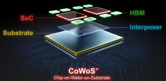
Figure: Schematic diagram of TSMC's CoWoS packaging technology structure
However, this technological advancement is not without its challenges. To achieve this, TSMC not only needs to break through the limitations of existing substrate sizes (e.g., 120 x 120 mm substrate size), but also faces significant challenges in system design layout. As the package size increases, issues such as power management and thermal efficiency will become new challenges. In the case of such a large package, how to ensure system stability, performance and reliability will have a direct impact on the viability and market acceptance of the technology.
1. Performance Enhancements and Market Impact
TSMC's 7,722 square millimeter CoWoS packaging technology is expected to deliver significant improvements in performance and capacity, mainly due to its ability to integrate more processor cores and memory. As the vertical stacking capability of chips in the 2nm and 1.6nm processes continues to increase, the number of transistors and the overall performance will also be greatly enhanced. For high-performance computing (HPC), artificial intelligence (AI), big data analysis and other fields, the promotion of this technology will bring revolutionary changes. It not only supports more complex data computing, but also meets the demand for massively parallel computing in the current AI boom.
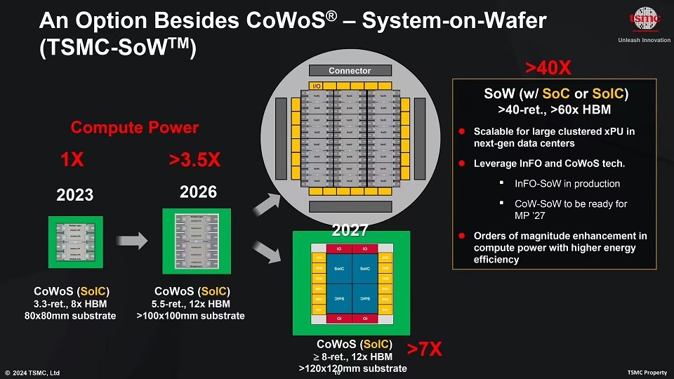
Figure: TSMC SoW is another SoC packaging option in addition to CoWoS
What's more, the successful implementation of this technology will also have a profound impact on the entire semiconductor industry. As the technology continues to mature, the demand for high-performance chips will further increase, especially in the fields of data centers, autonomous driving, 5G communications, and edge computing. TSMC's CoWoS technology will provide a more powerful and efficient hardware infrastructure for these fields, injecting new impetus into global scientific and technological innovation.
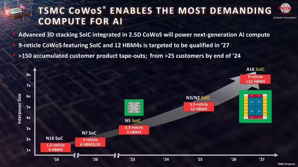
Figure: TSMC plans to upgrade CoWoS by 2027 to support 9x reticle and 12 HBM4 stacks
1. Future trends in packaging technology
According to the IDTechEx report, there will be several key trends in semiconductor packaging technology in the future, one of which is the application of larger interposer area. TSMC's CoWoS technology exemplifies this trend, enabling the integration of more processor cores and high-bandwidth memory (HBM) by providing a larger interposer area. This packaging solution will greatly improve the computing speed of the chip and meet the needs of high-speed data transmission and processing capabilities in AI, HPC and other fields.
In addition, TSMC is also actively developing compact universal photonic engine (COUPE) technology. This technology greatly reduces the resistance between the chips and improves the efficiency of data transmission by stacking electron dies with photonic dies on top of each other. The application of COUPE technology can effectively cope with the huge data transmission demand in AI applications and promote the further development of edge computing and cloud computing technologies.
With the explosive growth of global data traffic, TSMC's investment in next-generation packaging technology will become a bellwether for the industry. Through continuous technological breakthroughs, TSMC will not only achieve a leading edge in packaging technology, but also occupy an important position in a wider range of high-tech fields.
2. TSMC competes with global packaging technology
TSMC's CoWoS technology is not only a reflection of the company's internal innovation, but also a reflection of the competitive dynamics of the global semiconductor packaging market. At present, the world's major semiconductor manufacturers are continuously increasing their investment in advanced packaging technology, hoping to occupy a dominant position in the future technology competition. For example, Intel and Samsung are also actively developing their own packaging technologies, among which Intel's Foveros packaging technology and Samsung's H-BGA packaging solutions have made some progress in their respective application scenarios.
Although other manufacturers are also promoting the development of packaging technology, TSMC is still the leader in this field with its strong technology accumulation and accurate grasp of market demand. TSMC's increasing production capacity and innovation in packaging technology will bring more diversified solutions to the global semiconductor industry, and also promote the development of the market in the direction of more efficient and more integrated.
3. Summary
The release of TSMC's 7722 square millimeter CoWoS packaging technology marks a higher dimension of semiconductor packaging technology. This technological breakthrough not only provides a strong guarantee for hardware support in the fields of high-performance computing and artificial intelligence, but also promotes the comprehensive upgrade of the entire semiconductor industry in terms of performance, power consumption, and integration. With the official implementation of this technology in 2027, we have reason to believe that the future chip design will be more complex and efficient, injecting new vitality into the development of all walks of life.
Through continuous innovation, TSMC will continue to lead the trend of global semiconductor packaging technology and provide strong momentum for global technological development. With the rapid progress of science and technology, TSMC's CoWoS packaging technology will also become an important part of the semiconductor field, promoting the continuous evolution and transformation of the global semiconductor industry.


