

Cadence today announced a collaboration with TSMC to enhance the productivity and product performance of AI-driven advanced node designs and 3D-ICs. With the rapid adoption of AI applications, there is a growing demand for advanced silicon solutions that can handle huge data sets and high-performance computing. In response to this trend, the industry continues to innovate in advanced node silicon and 3D-IC technologies. TSMC and Cadence are at the forefront of this change, helping customers accelerate time-to-market while improving product performance.
TSMC has certified Cadence's industry leadership in digital and custom design flows, particularly in the implementation and signoff of its latest N3 and N2P process technologies. As a long-time DTCO partner, TSMC and Cadence have been working closely together to optimize the power, performance, and area (PPA) of the A16 chip and add advanced EDA features such as backside routing.
In addition, Cadence and TSMC have partnered on Cadence.AI to drive the next generation of AI-based digital and analog design automation to deliver superior productivity and quality of results. Cadence.AI is a chip-to-system AI platform that covers all aspects of design and verification. The cooperation between the two parties is mainly focused on the following three areas:
Cadence® Cerebrus™ Smart Chip Explorer: Apply AI to digital designs to optimize PPA.
Cadence's Joint Enterprise Data and Artificial Intelligence (JedAI) platform: Leverages generative AI for design debugging and analysis to power PPA analysis.
Cadence's Virtuoso® Studio: Enables the migration of traditional custom and analog designs to modern nodes, as well as circuit optimization and High Sigma Monte Carlo analysis.
The Cadence Integrity™ 3D-IC platform is a leading system-level discovery solution that unifies package, analog and digital implementations to provide a single-vendor platform for efficient 3D-IC design. This opens up new possibilities for innovation by supporting the latest 3Dblox features and constructs. To enable the ultra-high-density interconnect of TSMC's 3DFabric™ technology, the two companies are jointly developing the next generation of high-capacity baseframe routers to support chip-to-chip and chip-to-substrate connectivity.
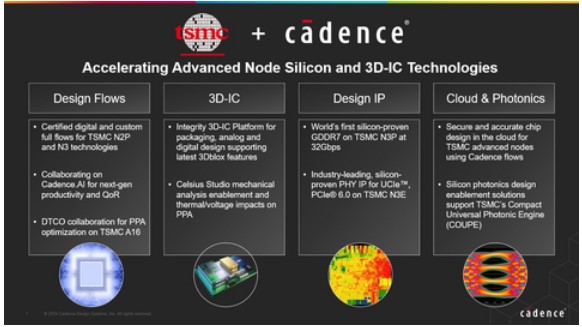
Figure: TSMC and Cadence have entered into a partnership
Multiphysics analysis and optimization are key to the successful implementation of 3D-IC technology. In addition to electrical and thermal analysis, TSMC and Cadence are collaborating on warpage and stress analysis for 3DFabric, and the results of Cadence's Celsius™ Studio analysis have been validated. The effects of heat and voltage on the power/IR/STA have also been enabled and validated for 3DFabric in the Cadence Integrity 3D-IC platform.
As the demand for data in AI factories continues to rise, so do the interconnection requirements, and the challenge of power limits becomes more prominent. Cadence offers a comprehensive portfolio of critical IP to efficiently move data between chips and data centers, including Universal Chip Interconnect Fast Lane ™ (UCIe™) 1.0, PCI Express® (PCIe®) 6.0 and the world's first silicon-proven GDDR7 running at speeds up to 32Gbps, providing the best price/performance for AI interfaces in the data center and at the network edge. To address the growing challenges of chip-to-chip communication, Cadence's silicon photonic design support solutions are also compatible with TSMC's compact Universal Photonic Engine (COUPE).
In addition, TSMC and Cadence's collaboration with automotive leaders makes IP development for current and future process nodes, such as TSMC N5A and later N3A, even more important as the amount of silicon in modern vehicle designs continues to increase.
The collaboration also demonstrates the accuracy and scalability that Cadence Cloud solutions provide to TSMC's advanced process nodes in the chip design flow from the front end to the back end. Through this partnership, customers can take advantage of Cadence's cloud-based solutions to significantly reduce design time.
"TSMC and Cadence have a long and successful partnership to bring global design to silicon reality," said Qinqi Teng, senior vice president and general manager of the Digital & Signoff Group at Cadence. Together, we're revolutionizing the future of silicon design with AI-driven EDA software that supports TSMC's latest process technology. We will continue to collaborate to deliver innovative solutions for next-generation technologies such as TSMC A16 and 3Dblox to help the AI factory of the future."
Dan Kochpatcharin, Head of Ecosystem & Alliance Management at TSMC, also said, "Through our partnership with Cadence, we have successfully enabled an AI-optimized design flow that drives advancements in N2 technology and 3D-IC design. This marks a major leap forward in digital versus custom solutions, paving the way for technological innovation in AI infrastructure.”


