

Yield Engineering Systems (YES) today announced that it has received a significant order from a leading Japanese semiconductor manufacturer to supply the VertaCure PLP system for its advanced packaging production line. These systems will play a key role in the manufacturing of AI and HPC solutions, especially in the field of 2.5D/3D packaging. YES products have built a strong reputation for excellence in curing, coating and annealing in R&D environments and large-scale production processes.
VertaCure PLP System: Efficient and automated vacuum curing technology
VertaCure PLP is a fully automated vacuum curing system that completely removes residual solvents, ensures uniform temperature distribution, and precisely manages heating and cooling rates. The advantages of the system also include no gas release after curing and excellent particle control. VertaCure PLP supports a variety of panel sizes, including 600 mm x 600 mm, 510 mm x 515 mm, and 300 mm x 300 mm, to meet different manufacturing needs.
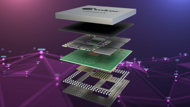
Figure: YES introduces the VertaCure PLP system, advancing advanced packaging technology for AI and HPC semiconductor solutions
Saket Chadda, senior vice president of the YES Drying Business Unit, said, "Today, AI and HPC solutions are shifting to chip-granular-based architectures that deliver higher performance, more memory, and better heat dissipation. As these solutions advance, the semiconductor industry is also moving to large panel-based substrates. He further noted, "To accommodate these large substrate sizes and increasing bandwidth demands, the semiconductor industry is adopting panel substrates. VertaCure PLP is a production-proven, automated, vacuum-curing system that offers excellent film performance and higher throughput than atmospheric curing systems. Its multi-zone temperature control system and laminar flow technology ensure the excellent uniformity and particle properties required for Polyimide, PBO and multilayer curing as well as bond annealing.”
Driving packaging technology innovation in AI and HPC applications
The VertaCure PLP system not only improves the efficiency of the curing process, but also improves the mechanical, thermal, and electrical properties of various polymers in wafer-level packaging, which are critical for AI and HPC applications. VertaCure PLP is a key technology to address the growing demand for high-performance, high-reliability curing systems as semiconductor packages move towards more complex 3D and 2.5D structures.
Alex Chow, Senior Vice President, Global Sales & Business Development, YES, said, "This important order further strengthens our leadership position in the curing tools market. Our VertaCure PLP product line is highly regarded for its controlled, repeatable, and scalable manufacturing processes in bonding and polymer curing applications. This system not only provides excellent quality, but also provides customers with an excellent total cost of ownership, especially in the semiconductor industry, especially for the production of advanced 2.5D and 3D packaging solutions.”
Summary
The launch of the VertaCure PLP system marks another important step forward for YES in semiconductor manufacturing, especially in advanced packaging applications for AI and HPC solutions. By providing efficient and reliable curing technology, YES is advancing the semiconductor industry in higher performance, larger package solutions. This not only meets the current semiconductor industry's demand for greater bandwidth and higher performance, but also lays a solid foundation for the advancement of AI and HPC-related technologies in the future.


